System parameters reference by all models
A development process in which all system parameters are stored in a central location and referenced by all models is possible. Using an integrated toolchain like PLECS helps to verify models for different purposes against each other and thus enables model continuity.
Simulation in practice
Simulations help developers in many ways during the development process of a new power electronics application.
The development process typically comprises of:
-
- Functional concept
- Component selection
- Mechanical design
- Controller implementation
- Test and verification under normal and faulty conditions.
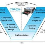
 V-model for the development process of a power electronic system
Typically, the development process refers to the V-model (above), where the design and implementation follow a top-down approach and the verification follows a bottom-up approach. At each level, the developed component is verified with appropriate test tools and procedures before being integrated into a larger system.
For the verification it is important that the same specifications are used as for the design. Although the design and verification tools may use models with different levels of detail, it is important to ensure that the models produce comparable results.
Phase #1 – circuit concept
In the first phase of a new design, the feasibility of a power circuit and a proper control scheme can be assessed quickly with ideal circuit components and generic control blocks. During this conceptual phase, no manufacturer-specific information is needed to model the individual components of a power converter. Rather, power semiconductors such as MOSFETs and diodes can be represented by simple on/off switches that correspond to their functional behaviour. The parasitic properties of passive components like winding resistance and inductor saturation can be neglected unless they play a functional role for the circuit operation.
Likewise, the controls are represented by functional block diagrams or state machines, independent of their final implementation. These controls may later be realised as analogue circuitry, digital logic, microcontroller code or hardware PWM generators.
Simulation software used in the conceptual phase must provide generic models for all types of electrical components encountered in power electronic applications. As power semiconductors are normally operated in switch mode they should be modelled as ideal switches to reduce the complexity of the simulation model. The user must be able to freely connect arbitrary components and to create his own customised components by means of subsystems.
During the conceptual phase, the system model can grow in complexity and size. In order to obtain fast transient simulations without significant integration errors, the use of a variable time-step solver is strongly recommended. A variable step solver automatically steers the time step in such a way that the maximum integration error is not exceeded and switching instants and other discontinuous events are hit exactly.
Phase #2 – component selection
Based on the current and voltage requirements, components are selected and the mechanical layout is created. In this second phase, simulations help predict the thermal losses and the resulting temperatures. The thermal domain computes the losses generated by the electrical circuit and models the heat transfer.
Switching and conduction losses can be simulated efficiently using a set of loss tables for each semiconductor. Tables for switching losses provide the dissipated energy depending on the blocking voltage, the on-state current and the junction temperature of the device. Tables for computing conduction losses show the voltage drop as a function of on-state current and device temperature. In each simulation step, the thermal losses can be calculated and fed into a thermal equivalent network that comprises the semiconductor device, the heat sink and the external cooling arrangement.
Loss tables v simulated voltage and current transients
The advantage of loss tables over simulating voltage and current transients during switching is that ideal switching (and therefore high simulation speed) is maintained. The computation of the thermal domain adds some extra work to the electrical simulation based on ideal components. Power semiconductor loss tables are readily available from a growing number of semiconductor manufacturers.